- 您现在的位置:买卖IC网 > Sheet目录2005 > LTC2262CUJ-14#TRPBF (Linear Technology)IC ADC 14BIT 150MSPS 40-QFN
LTC2262-14
22
226214fc
For more information www.linear.com/LTC2262-14
APPLICATIONS INFORMATION
Of particular importance is the 0.1F capacitor between
REFH and REFL. This capacitor should be on the same
side of the circuit board as the A/D, and as close to the
device as possible (1.5mm or less). Size 0402 ceramic
capacitors are recommended. The larger 2.2F capacitor
between REFH and REFL can be somewhat further away.
The VCM capacitor should be located as close to the pin
as possible. To make space for this the capacitor on VREF
can be further away or on the back of the PC board. The
traces connecting the pins and bypass capacitors must be
kept short and should be made as wide as possible.
The analog inputs, encode signals, and digital outputs
should not be routed next to each other. Ground fill and
grounded vias should be used as barriers to isolate these
signals from each other.
HEAT TRANSFER
MostoftheheatgeneratedbytheLTC2262-14istransferred
from the die through the bottom-side exposed pad and
package leads onto the printed circuit board. For good
electricalandthermalperformance,theexposedpadmust
be soldered to a large grounded pad on the PC board.
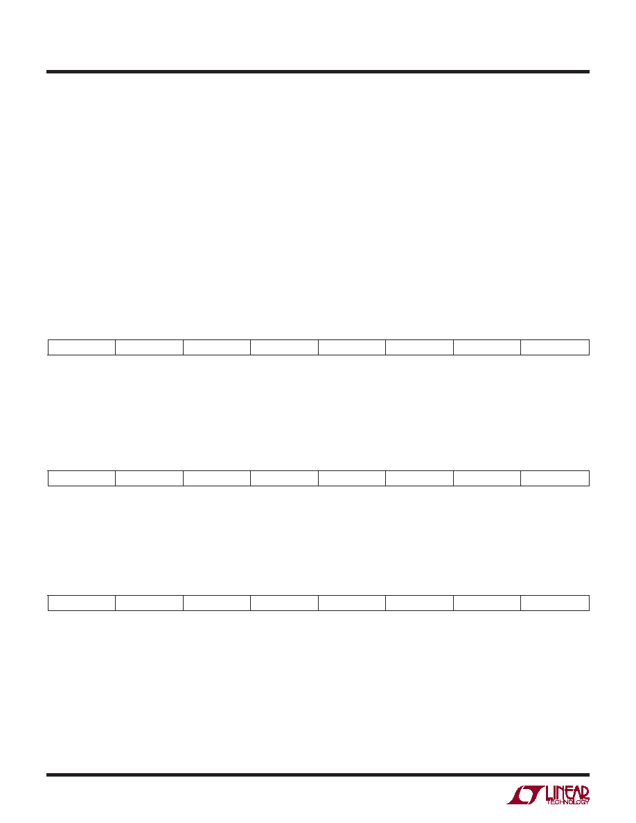
Table 3. Serial Programming Mode Register Map
REGISTER A0: RESET REGISTER (ADDRESS 00h)
D7
D6
D5
D4
D3
D2
D1
D0
RESET
X
Bit 7
RESET
Software Reset Bit
0 = Not Used
1 = Software Reset. All Mode Control Registers are Reset to 00h. This Bit is Automatically Set Back to Zero at the end of the SPI write
command
The reset register is write only
Bits 6-0
Unused, Don’t Care Bits.
REGISTER A1: POWER-DOWN REGISTER (ADDRESS 01h)
D7
D6
D5
D4
D3
D2
D1
D0
X
PWROFF1
PWROFF0
Bits 7-2
Unused, Don’t Care Bits.
Bits 1-0
PWROFF1:PWROFF0
Power Down Control Bits
00 = Normal Operation
01 = Nap Mode
10 = Not Used
11 = Sleep Mode
REGISTER A2: TIMING REGISTER (ADDRESS 02h)
D7
D6
D5
D4
D3
D2
D1
D0
X
CLKINV
CLKPHASE1
CLKPHASE0
DCS
Bits 7-4
Unused, Don’t Care Bits.
Bit 3
CLKINV
Output Clock Invert Bit
0 = Normal CLKOUT Polarity (As Shown in the Timing Diagrams)
1 = Inverted CLKOUT Polarity
Bits 2-1
CLKPHASE1:CLKPHASE0
Output Clock Phase Delay Bits
00 = No CLKOUT Delay (As Shown in the Timing Diagrams)
01 = CLKOUT+/CLKOUT– Delayed by 45° (Clock Period 1/8)
10 = CLKOUT+/CLKOUT– Delayed by 90° (Clock Period 1/4)
11 = CLKOUT+/CLKOUT– Delayed by 135° (Clock Period 3/8)
Note: If the CLKOUT Phase Delay Feature is Used, the Clock Duty Cycle Stabilizer Must Also be Turned On
Bit 0
DCS
Clock Duty Cycle Stabilizer Bit
0 = Clock Duty Cycle Stabilizer Off
1 = Clock Duty Cycle Stabilizer On
发布紧急采购,3分钟左右您将得到回复。
相关PDF资料
LTC2262IUJ-12#PBF
IC ADC 12BIT 150MSPS 40-QFN
LTC2264CUJ-12#PBF
IC ADC 12BIT SER/PAR 40M 40-QFN
LTC2268IUJ-14#TRPBF
IC ADC 14BIT 125MSPS DUAL 40QFN
LTC2280CUP#PBF
IC ADC DUAL 10BIT 105MSPS 64-QFN
LTC2281IUP#PBF
IC ADC 10BIT DUAL 64-QFN
LTC2282CUP#PBF
IC ADC DUAL 12BIT 105MSPS 64-QFN
LTC2284CUP#PBF
IC ADC DUAL 14BIT 105MSPS 64-QFN
LTC2285CUP#PBF
IC ADC DUAL 14BIT 125MSPS 64QFN
相关代理商/技术参数
LTC2262IUJ-12#PBF
功能描述:IC ADC 12BIT 150MSPS 40-QFN RoHS:是 类别:集成电路 (IC) >> 数据采集 - 模数转换器 系列:- 标准包装:1 系列:- 位数:14 采样率(每秒):83k 数据接口:串行,并联 转换器数目:1 功率耗散(最大):95mW 电压电源:双 ± 工作温度:0°C ~ 70°C 安装类型:通孔 封装/外壳:28-DIP(0.600",15.24mm) 供应商设备封装:28-PDIP 包装:管件 输入数目和类型:1 个单端,双极
LTC2262IUJ-12#TRPBF
功能描述:IC ADC 12BIT 150MSPS 40-QFN RoHS:是 类别:集成电路 (IC) >> 数据采集 - 模数转换器 系列:- 标准包装:1 系列:- 位数:14 采样率(每秒):83k 数据接口:串行,并联 转换器数目:1 功率耗散(最大):95mW 电压电源:双 ± 工作温度:0°C ~ 70°C 安装类型:通孔 封装/外壳:28-DIP(0.600",15.24mm) 供应商设备封装:28-PDIP 包装:管件 输入数目和类型:1 个单端,双极
LTC2262IUJ-14#PBF
制造商:Linear Technology 功能描述:ADC Single Pipelined 150Msps 14-bit Parallel/LVDS 40-Pin QFN EP 制造商:Linear Technology 功能描述:IC ADC 14BIT 1.8V 150MSPS 40-QFN
LTC2262IUJ-14#TRPBF
制造商:Linear Technology 功能描述:ADC Single Pipelined 150Msps 14-bit Parallel/LVDS 40-Pin QFN EP T/R 制造商:Linear Technology 功能描述:IC ADC 14BIT 150MSPS 40-QFN
LTC2263-12
制造商:LINER 制造商全称:Linear Technology 功能描述:12-Bit, 65Msps/40Msps/25Msps Low Power Dual ADCs
LTC2263-14
制造商:LINER 制造商全称:Linear Technology 功能描述:Quad 14-Bit, 125Msps ADC with Integrated Drivers
LTC2263CUJ-12#PBF
功能描述:IC ADC 12BIT SER/PAR 25M 40-QFN RoHS:是 类别:集成电路 (IC) >> 数据采集 - 模数转换器 系列:- 标准包装:1 系列:microPOWER™ 位数:8 采样率(每秒):1M 数据接口:串行,SPI? 转换器数目:1 功率耗散(最大):- 电压电源:模拟和数字 工作温度:-40°C ~ 125°C 安装类型:表面贴装 封装/外壳:24-VFQFN 裸露焊盘 供应商设备封装:24-VQFN 裸露焊盘(4x4) 包装:Digi-Reel® 输入数目和类型:8 个单端,单极 产品目录页面:892 (CN2011-ZH PDF) 其它名称:296-25851-6
LTC2263CUJ-12#PBF
制造商:Linear Technology 功能描述:IC ADC 12BIT 25MSPS QFN-40